Additive manufacturing (AM) is a family of bottom-up technologies
that may answer to necessities, supporting the rapid fabrication of components with
complex shapes.
The most well-known advantages of additive manufacturing are flexibility in the
part design, possibility of realizing light parts, mechanical properties higher
than those of conventionally casted materials and integration of different functionalities.
Among the industrial AM technologies, selective laser melting
(SLM) is the most widespread, thanks to its process stability and its favorable
ratio between costs and part quality.
However, selective laser melted products require post-processing,
like
- heat treatments for stress relieving,
- finishing for improving surface quality and controlling dimensional tolerances,
- coatings for functionalizing the surface with extra properties.
The three-step process
The study of the entire production route, including SLM process, heat treatments
and depositions of functional thin films, can lead to obtain printed ready-to-use
tools with potential complex shapes and high degree of customization.
In this article we’ll see how thin film deposition process can be carried out
to coat titanium substrates, realized via Selective Laser Melting.
Read on to get a comprehensive answer to the following questions.
Is it possible to coat the titanium alloy substrates to obtain a good improvement
of the mechanical surface features?
What’s the role of vacuum heat treatments on additive manufactured parts?
Can the laser scanning paths affect the resulting adhesion of the coatings?
And much more…
Step 1: selective laser melting
SLM is a powder bed process, in which a scanning laser beam can melt locally
a limited portion of powder on the current layer. The process is replicated for
several layers, therefore giving rise to near net shape 3D parts, manufactured through
a layer by layer building strategy.
Thanks to the limited liquid pool size, very high cooling rates are induced and
this allows obtaining fine microstructures.
Regarding the availability of materials which can be processed via selective
laser melting, Titanium64 alloy (Ti6Al4V) has a good process-ability
and is a widespread material employed in several fields, such as the biomedical
and the aerospace ones.
We’re going to produce cylindrical samples from commercial Ti6Al4V powder by
means of a selective laser melting 3D printer (mod. AM400 from
Renishaw, installed at the Lecco headquarters of the CNR ICMATE).
The adopted process parameters are listed in the following table.
| Scanning strategy |
Power |
Exposure time |
Layer thickness |
Point/hatch distance |
Platform temperature |
Atmosphere |
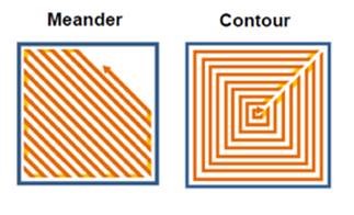
| Meander |
200W |
50µs |
30µm |
75µm |
30°C |
Argon |
| Contour |
100W |
60µs |
30µm |
75µm |
30°C |
Argon |
Three-dimensional topological characterization by means of a stylus profiler
(Bruker, Dektat XT), has been carried out on different substrate surfaces, in order
to evaluate the geometrical features of SLM prepared samples and identify the optimal
scanning scheme suitable for the subsequent HiPIMS deposition.
We tested 2 different scanning design to realize the samples, meander and contour.
Later in this article we will see how this has led to interesting results.
Did you like this article up to here?
Before you continue, follow us on our Twitter page pressing the button here below!
In this way, we'll be able to keep you updated on most advanced technologies for heat treatments not only with our posts, but also with the best articles that we collect around the web.
Step 2: substrate vacuum thermal treatments
Selective laser melted substrates were heat treated with a TAV H3 all
metal vacuum furnace at 950°C for 1 hour in order to evaluate how the resulting
material structure and microstructure changings could affect the thin film growth
and, consequently, their mechanical properties.
The thermal treatments were carried out in high vacuum (around
10-5-10-6 mbar).
Step 3: thin film deposition process
Physical Vapor Deposition High-Power Impulse Magnetron Sputtering
(PVD HiPIMS) represents an evolution of the conventional magnetron sputtering technique
and permits the depositions of high quality, dense, adherent coatings onto substrates
with complex shapes.
Moreover, for their excellent wear and corrosion resistance properties,
AlTiN hard films are widely used in many applications such as
cutting tools, aero-engine sector, bio-implants, etc.
In this work, the effect of AlTiN hard coatings on AMed Ti6Al4V flat samples
on microstructural and mechanical properties were investigated. The microstructure
and the mechanical response of the deposited films were characterized through Scanning
Electron Microscopy (SEM), X-Rays Diffraction (XRD) and nanoindentation testing.
A closer look at the coating process
The conditions of PVD HiPIMS deposition process were adjusted in order to optimize
the matching between the metallic substrate and the ceramic coating.
The protective thin films were deposited by reactive PVD HiPIMS onto doped Si
(100) slides (Si-Mat), polished Ti6Al4V disks (obtained from a commercial titanium
alloy billet with a final cylinder shape having a diameter of 25 mm and a thickness
of 4 mm), and polished meander selective laser melted substrates (before and after
vacuum thermal treatment).
- The polishing process carried out for some of titanium
alloy samples was performed with a colloidal silica suspension (OP-U, 0.04 µm,
Struers) employing Tegramin 20 polishing machine (Struers).
The substrates were then sonicated in ethanol and isopropanol and dried with
N2 (99.998%).
- The sputtering process was carried out starting from a
base pressure of 5.0×10⁻⁷ mbar, employing a AlTi target (50:50 at%,
99.9 % pure, with diameter of 50.8 mm, purchased by MaTek), under a total working
pressure of 5.0 x 10⁻³ mbar, in atmosphere consisting of a mixture
of Ar (99.9997%) with several partial pressure of N2 (pN2,
99.998%), such as 14%, 20%, 25%, and 30%.
- The deposition process was driven by a Ionautics Hipster
6 power supply maintaining constant power density (15 W cm-2), frequency
(1500 Hz), pulse time (50 µs), substrate bias supplied by Ionautics Hipster
1 (-50 V power, frequency 1500 Hz, pulse time 100 µs, synchronized), temperature
(350°C), and the substrate-target distance (60 mm).
The data collection
Let's collect experimental results on microstructural and mechanical characterizations.
The structure, the composition, and the mechanical features of thin films were
investigated by X-ray Diffraction (XRD), Energy Dispersive Spectroscopy (EDS) associated
to Field Emission Scanning Electron Microscopy (FE-SEM), and nanoindentation. Finally,
FE-SEM was also employed for evaluating microstructure evolution of both substrates
and thin films.
If you are interested in the tools used for the acquisition of experimental data,
read here below, otherwise you can jump directly to the next chapter.
- X-ray diffraction profiles of the samples were obtained
using a Philips PW 3710 X-Ray diffractometer with Bragg-Brentano geometry and
a CuKα source (40 kV, 30 mA). Phase identification on the XRD profiles was carried
out employing Match! software, exploiting inorganic crystal structure database.
- The morphological and quantitative compositional characterizations
were performed by Sigma Zeiss field emission scanning electron microscope equipped
with Oxford X-Max energy dispersive X-Ray spectroscopy (EDS) system. The EDS
point analyses were carried out onto AlTiN films deposited at 20 kV accelerating
voltage, with acquisition time of 50 seconds, employing software INCA 4.14 (Oxford
Instruments).
For these analyses, films were deposited onto monocrystalline doped Si slides
with a thickness over than 2 µm for having a perfectly planar and conductive
substrate, in order to minimize the errors due to the surface morphology and
the influence of substrate nature, and thus making the quantification assessment
reliable.
The software was calibrated for quantification, referencing the standards to
Co optimization standard, with polished BN, as standards for N, Al and Ti. The
empirical formulas were calculated maintaining the number of N atoms fixed to
1.0 and the respective errors were calculated as the standard deviations of
the measurements.
- Hardness and elastic modulus values were measured by instrumented
nanoindentation, with Nanotest system (Micromaterials, Wrexham, UK) equipped
with a Berkovich tip.
Tests were performed in depth control mode, and the maximum depth was selected
so that the ultimate penetration depth of each indent was less than 10% of the
mean film thickness, in order to minimize the influence of the substrate on
the measurements.
Data were obtained by statistical analysis of 25 indentations for each sample
surface, arranged on square grids. The nano-hardness and the elastic modulus
were estimated by applying the Oliver and Pharr method at the resultant load–displacement
curves.
Conclusions
Now we’re ready to analyse the data of the additive manufacturing and coating
processes.
Do not miss the next article, we’ll answer many unsolved questions, giving you a
broad overview of the possibilities offered by these new technologies.
National Research Council; Institute of Condensed Matter Chemistry and Technologies
for Energy (Padova): S. Battiston, F. Montagner, V. Zin
National Research Council; Institute of Condensed Matter Chemistry and Technologies
for Energy (Lecco): C.A. Biffi, J. Fiocchi, A. Tuissi
TAV VACUUM FURNACES SpA: A. Fiorese, A. Gionda
Did you like the article?
Subscribe to our Telegram channel and stay up to date on most advanced technologies for heat treatments.

Don't you have Telegram?
If you do not have Telegram yet, use one of the following buttons to install it: